How to Deploy Edge AI on FPGAs with Familiar Tools
Contributed By DigiKey's North American Editors
2026-02-17
Artificial intelligence (AI) at the network edge (edge AI) rarely means just inference alone. Real-world deployments typically involve high-speed input/output (I/O), signal conditioning, and real-time control loops, all of which execute concurrently. These multi-function workloads demand tight coordination and levels of determinism that designers find challenging to meet using mainstream AI hardware.
Two factors compound the issue. First, AI models are evolving at a breakneck pace, pushing designers to adopt platforms that support rapid algorithm updates. At the same time, many edge systems stay in the field for a decade or longer, making it difficult to ensure long-term adaptability. Second, the path from trained model to deployed system remains fragmented. Data scientists work in PyTorch and TensorFlow, while embedded teams use entirely different toolchains, creating friction during handoffs that slows time to production.
Meeting these challenges requires platforms that combine high-throughput AI processing with deterministic behavior, flexible I/O, and long-term adaptability, all within constrained power envelopes typical of edge deployments.
This article highlights the applications and associated requirements that challenge designers to explore new edge AI architectures. It then introduces edge AI-enabled field-programmable gate array (FPGA) devices and software tools from Altera and shows how they can be used to meet the needs of these applications across a wide range of performance and power points.
Edge AI evolution demands architectural innovation
Edge systems increasingly employ diverse AI techniques, classic machine learning (ML) for anomaly detection, convolutional neural networks (CNNs) for perception, and transformers for large language models (LLMs). These compute-intensive algorithms often coexist with demanding non-AI functions, such as signal processing, networking, and real-time control.
Autonomous systems are a prime example. They often need to ingest data from multiple sensor modalities (e.g., video, audio, radar, LiDAR, and motion/position feedback), pre-process those streams at high throughput, analyze the results with sophisticated AI, and then manage high-precision control loops, all with reliable determinism.
Many similar examples can be found across industrial automation, medical imaging, defense, and telecommunications applications. A common theme is that the converging workloads are challenging to accommodate with traditional architectures.
How FPGAs are uniquely suited to edge AI
In contrast, these requirements map well to FPGAs' capabilities. At their core, FPGAs provide configurable logic that executes operations in true parallel, with timing behavior baked in at design time rather than fluctuating during runtime. This architecture enables the low-latency determinism critical to edge AI. The flexible logic also leverages powerful I/O: FPGAs generally offer a wealth of high-speed I/O that can interface with a wide range of sensors and actuators, providing tight coupling with AI processing.
FPGAs also contain distributed internal memory, which keeps data close to the logic that operates on it. This reduces the bottlenecks that arise when multiple processing stages must compete for access to a shared memory bus, a common constraint in processor-based architectures.
Many FPGAs also incorporate specialized digital signal processing (DSP) hardware. These hardened circuits deliver higher performance and better power efficiency for signal-processing workloads than the general-purpose fabric. Some FPGAs also integrate hardwired processor systems that can run standard software stacks, including Linux, enabling conventional software development for tasks like networking, device management, and user interfaces.
In short, a single FPGA can consolidate functions that might otherwise require separate I/O chips, AI accelerators, DSP, and control-plane processors. The result can be a reduced bill of materials (BOM), a smaller board footprint, and lower power consumption, while maintaining the low latency and determinism that edge AI applications demand.
How the addition of AI tensor blocks unlocks new possibilities
Traditional FPGA DSP hardware is already well-suited to many edge workloads, but AI inference tends to be dominated by dense but low-precision multiply-accumulate operations. To address this, Altera’s Agilex 3 and Agilex 5 devices feature Enhanced DSP with AI tensor blocks. This is specialized hardware for matrix-matrix and vector-matrix multiplications, which appear repeatedly in AI compute graphs.
At the heart of this approach is a scalar product and adder/accumulator engine (Figure 1). In tensor mode, the hardwired dot engine performs a 10-element dot product using 8-bit inputs and preloaded 8-bit weights. To extend dynamic range, the data path can also use a shared “common exponent” for block floating-point-style scaling, addressing the typical scenario in which AI inference requires high dynamic range but low precision.
 Figure 1: The AI tensor block can perform 10-element dot products. (Image source: Altera)
The dot-product result is 32 bits (fixed-point or single-precision floating-point), and it can be cascaded to an additional adder/accumulator stage to compute larger dot products across adjacent blocks. Each AI tensor block includes two dot-product columns, enabling a variety of operating modes.
In a typical use case, some of the enhanced math hardware is used in its traditional DSP role, such as performing fast Fourier transforms (FFTs) on radar data. Others are used as AI tensor blocks, such as a CNN to perform object detection. This flexibility is critical for edge systems that must handle AI alongside other compute-intensive functions.
A range of FPGA options for different AI workloads
The Agilex families also provide considerable flexibility in performance scaling. Parts range from efficiency-focused devices measuring just 12 mm × 12 mm to high-performance variants delivering up to 152.6 peak tera operations per second (TOPS), with similar scaling in I/O and memory interface capabilities.
An example of a high-performance part is the Agilex 5 A5ED065BB32AE4SR0, which delivers 22.17 TOPS in a 32 × 32 mm package. An example of an efficiency-oriented part is the Agilex 3 A3CW135BM16AE6S, which provides 2.8 TOPS in a 16 × 16 mm package. Key specifications for each are shown in Table 1.
|
Table 1: Shown are some key specifications for sample Agilex 5 and Agilex 3 FPGAs. (Table source: Altera (modified by author))
Both families are available as traditional FPGAs or as systems-on-chip (SoCs) with integrated Arm processors. Agilex 3 SoCs incorporate a dual-core, 800 megahertz (MHz), Arm Cortex-A55. Agilex 5 SoCs feature an asymmetric cluster with dual 1.8 gigahertz (GHz) Cortex-A76 cores alongside dual 1.5 GHz Cortex-A55 cores. Both configurations support Linux, enabling conventional software development for networking, device management, and user interfaces.
Simplifying edge AI deployment using FPGAs
AI models are typically developed in software-centric frameworks with rapid iteration cycles, while FPGA implementations historically required hardware development skills and longer integration cycles. Altera’s FPGA AI Suite (Figure 2) provides a more direct path from a trained model to deployable FPGA inference intellectual property (IP) using a flow compatible with industry-standard AI tooling.
") Figure 2: The FPGA AI Suite workflow bridges standard AI frameworks to FPGA deployment. (Image source: Altera)
Figure 2: The FPGA AI Suite workflow bridges standard AI frameworks to FPGA deployment. (Image source: Altera)
The workflow can be summarized as follows:
- Develop the inference model in a standard framework such as PyTorch, TensorFlow, or ONNX.
- Use the OpenVINO toolkit to convert the model into an intermediate representation (IR) comprising a graph file (.xml) and weights (.bin).
- Pass the IR artifacts into the FPGA AI Graph Compiler, which maps the model onto the available FPGA resources. Such resources can include an external host processor, an internal processor, or a headless configuration.
- Compile and deploy the resulting layers using Quartus Prime Pro Edition, with execution managed through the inference engine runtime stack and FPGA AI application programming interfaces (APIs) for memory movement and hardware scheduling.
- As part of the compilation process, use the Architecture Optimizer to balance performance and resource usage. For example, use it to ensure the implementation meets inference-throughput goals while leaving room for other FPGA logic.
In practical terms, this approach's value is that it turns “deploy on an FPGA” into an integration process rather than an accelerator design effort. Data scientists can stay within established model-development workflows, while FPGA and embedded teams receive artifacts that naturally fit into a build-and-deploy cycle, enabling faster iteration as models and requirements evolve. Pre-trained models available through the Open Model Zoo for OpenVINO toolkit can further accelerate development.
Getting a quick start with easy-to-use development kits
To start exploring edge AI on FPGAs, designers have several development kit options. For higher-performance applications, the Terasic P0775 Atum A5 Development Kit (Figure 3) is a good choice. Built around the Agilex 5 A5ED065BB32AE4SR0, the kit provides a broad mix of interfaces suited to edge-class systems. Key features include 8 gigabytes (Gbytes) of DDR4, QSFP+ and 2.5 gigabit (Gbit) Ethernet (GbE) ports, PCIe Gen 3 x4, dual MIPI camera connectors, and an HDMI output. The kit includes a free license for Quartus Prime Pro Edition.
 Figure 3: The P0775 Atum A5 Development Kit provides access to high-performance AI and vision development. (Image source: Terasic)
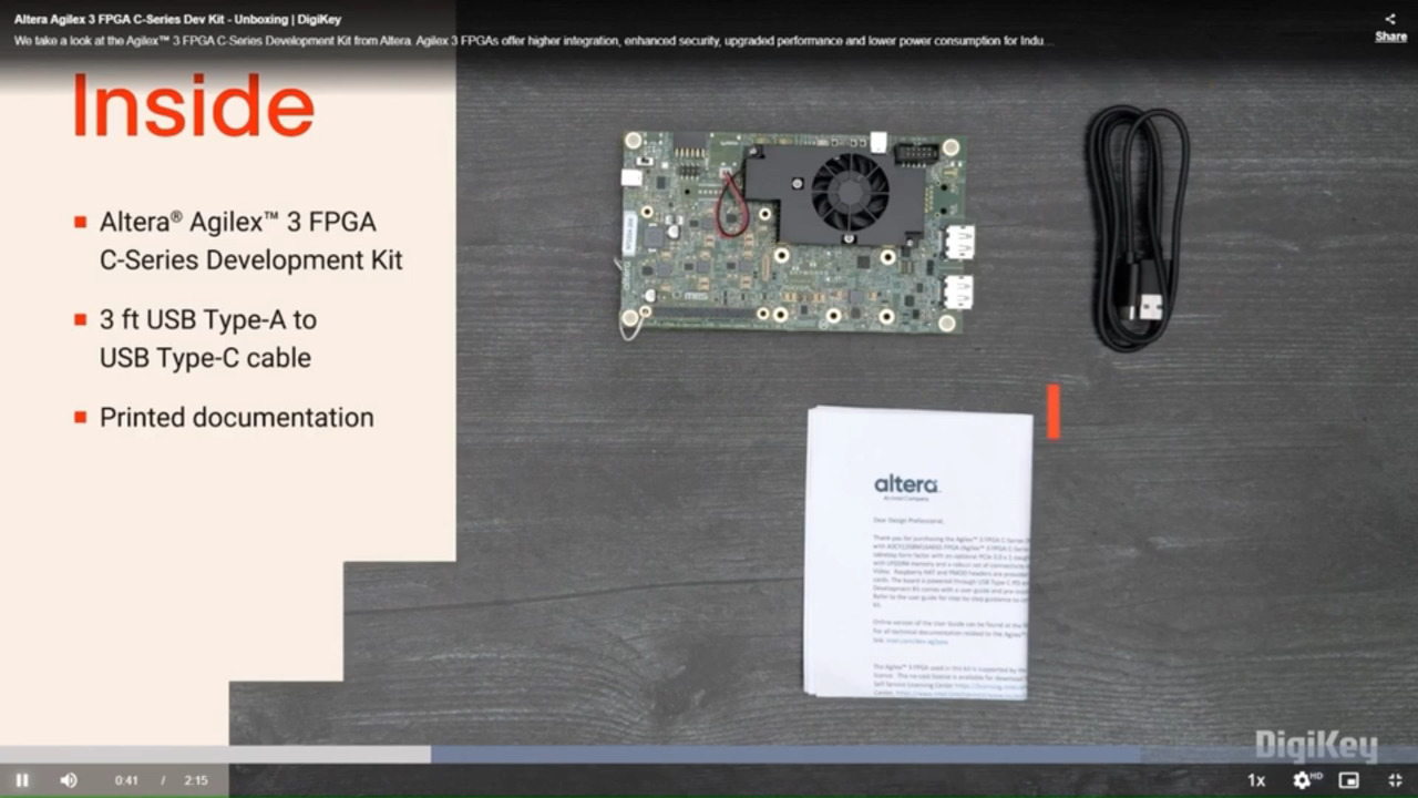
For efficiency-focused applications, designers can turn to the DK-A3W135BM16AEA Agilex 3 FPGA and SoC C-Series Development Kit (Figure 4). Built around the Agilex 3 A3CW135BM16AE6S, this kit emphasizes compact prototyping with ecosystem-friendly expansion. The board provides 4 Gbytes of LPDDR4, GbE, DisplayPort, and USB 2.0, along with a Raspberry Pi HAT connector and a Digilent Pmod interface for low-friction expansion.
 Figure 4: The DK-A3W135BM16AEA Agilex 3 FPGA and SoC C-Series Development Kit provides a compact platform for efficiency-focused edge AI. (Image source: Altera)
Conclusion
The introduction of LLMs and other novel AI workloads at the edge is prompting developers to seek new approaches. FPGAs offer a unique solution that not only provides low-latency, deterministic performance but also handles many other system functions. With AI-enabled Agilex FPGAs and the FPGA AI Suite, developers can access these capabilities quickly and easily, opening new architectural possibilities for highly adaptive, long-lived designs.
Disclaimer: The opinions, beliefs, and viewpoints expressed by the various authors and/or forum participants on this website do not necessarily reflect the opinions, beliefs, and viewpoints of DigiKey or official policies of DigiKey.